Interconnects are essential to future nanoelectronic devices, which provide the electrical paths needed in a circuit to pass signals and data between different functional blocks. Thus, how to select suitable nanowries (NWs) for interconnects is a hot topic. In the semiconductor industry, copper is widely used due to its superior electrical and thermal conductivities. However, copper NWs are quite unstable and easily oxidated in a short period, and thus their practical application is restricted.
In recent years, progresses have been made in the study of electrical transport properties of single Cu@C nanocable, electrical properties of T-shaped SnO2 nanowires and conduction mechanism of individual cross-junction SnO2 nanobelts by the research group which is under the supervision of Prof. Jinhuai Liu and Prof. Xingjiu Huang, one of the international renowned scholars at research center for biomimetic functional materials and sensing devices, Institute of Intelligent Machines, Chinese Academy of Sciences (Materials Today, 2011, 14, 42;Small, 2012, 8, 53;Small, 2013, 9, 2678).
Based on the achievements above, the research group further adopted a method to synthesize Cu NWs through a hydrothermal route with the reduction of copper chloride using octadecylamine (ODA). The reasons for their environmental stability could be due to the interaction of ODA+ molecules with the surface of Cu NWs, and thus strong N-Cu chemical bonds are formed. Additionally, X-ray absorption fine structure (XAFS) spectroscopy was conducted to confirm the formation of N-Cu bonds at the interface between Cu NW and ODA+ molecules. The presence of N-Cu bonds on the surface of Cu NWs would greatly restrain the oxidation process. A type of nanodevice constructed from individual Cu NW was fabricated by a focused-ion-beam (FIB) deposition technique. Four-probe measurement was applied to the investigation of the electrical transport properties of individual Cu NW, and the results showed that the temperature-dependent resistance of the Cu NW was fairly linear in the temperature range from 25 K to 300 K, and the Cu NW retained low resistivity of approximately 3.5×10⁻⁶Ω.cm, in the same order as that of bulk copper. Furthermore, in situ bending measurements were carried out to quantitatively assess the response of individual Cu NWs to external loading by a force measurement system (FMS, Kleindiek, Germany) inside a SEM system, which indicated that the mechanical strength decreased with the decreasing diameters, and the small size Cu NWs tend to be brittle and elastic while the large size NWs showed some extent ductility. The study showed that the Cu NWs could act as ideal nanoscale building blocks for interconnects in future nanoscale devices. The experimental results were published in ACS Nano (ACS Nano 2015, 9, 241-250).
This research was supported by the National Basic Research Program of China (2011CB933700, and 2011CB921404), and the Strategic Priority Research Program (B) of the CAS (XDB01020000).
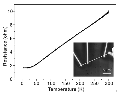
Figure 1. The Cu NWs show excellent electrical transport properties in the temperature range of 5-300K, and the room-temperature resistivity of the Cu NW is near that of the bulk copper.
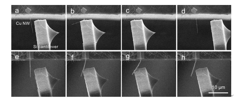
Figure 2. Consecutive SEM images of an individual Cu NW with a diameter of about 80 nm (a - d) and 300 nm (e - h), respectively, during different bending stages.